


")


Thin/Ultrathin BBO Crystals


BBO crystal is by far the most useful nonlinear crystal for frequency conversions of ultrafast lasers. One of the main considerations for ultrafast applications is pulse broadening induced by the group velocity (Vg) mismatch between the input pulses and the generated pulse due to the dispersion in the crystal. In order to avoid pulse broadening, the thickness of the crystal should not exceed the maximum length Lmax as defined by the pulse width divided by the inversed group velocity mismatch (IGVM = ΔVg-1). In the table below are the Lmax for second harmonic generation (SHG) and sum frequency generation (SFG) of 10 fs pulses in the wavelength range of a common Ti:Sapphire laser,
| Type I PM in BBO | SHG @ 700 nm |
SHG @ 800 nm |
SHG @ 900 nm |
SFG @ 700 + 350 nm |
SFG @ 800 + 400 nm |
SFG @ 900 + 450 nm |
| IGVM (ps/cm) | 2.72 | 1.92 | 1.40 | 8.50 | 5.68 | 4.08 |
| Lmax @10 fs (µm) | 40 | 50 | 70 | 10 | 18 | 25 |
A thickness of sub-100 µm (0.1 mm) is apparently desired for all the frequency conversion processes of 10 fs pulses. In particular, crystals as thin as 10-20 µm may be needed for generation of very short UV wavelengths below 300 nm.
Newlight Photonics offers on this page ultrathin/thin BBO crystals 10 µm (0.01 mm) - 3.0 mm thick developed for frequency conversions of short pulses. The typical apertures are 5x5 mm, 6x6 mm, 10x10 mm, 12x12 mm, and 15x15 mm. The maximum aperture available at this time is 20x20mm.
We also supply birefringent calcite plates and alpha-BBO plates for compensation of the temporal walkoff in BBO crystals (time delay compensators).
For thicker BBO crystals (T>3 mm) used for longer pulses (ns, ps), please visit Thick BBO Crystals.
| Part No. | Description | Application | Aperture | Thickness | Price | Availability | Add to Cart |
Structural and Physical Properties:
| Crystal Structure | Trigonal, space group R3c, Point group 3m |
| Cell Parameters | a = b = 12.532 Å, c = 12.717 Å, Z = 6 |
| Melting Point | 1095 °C |
| Transition Temperature | 925 °C |
| Mohs Hardness | 4 |
| Density | 3.85 g/cm3 |
| Specific Heat | 1.91 J/cm3 x K |
| Hygroscopic Susceptibility | Low |
| Thermal Expansion Coefficients | a, 4 x 10⁻⁶ /K; c, 36 x 10-6 /K |
| Thermal Conductivity | ⊥c, 1.2 W/m/K; //c, 1.6 W/m/K |
Linear Optical Properties:
| Transparency Range | 189-3500 nm |
| Optical Homogeneity | δn ~ 10-6 /cm |
| Absorption Coefficient | < 0.1% /cm (at 1064 nm) |
| Sellmeier Equations (λ in µm) |
no2=2.7359+0.01878/(λ2-0.01822)-0.01354λ2 ne2=2.3753+0.01224/(λ2-0.01667)-0.01516λ2 |
|
Refractive Indices |
no = 1.6545, ne = 1.5392 no = 1.6606, ne = 1.5444 no = 1.6742, ne = 1.5547 no = 1.6930, ne = 1.5679 no = 1.7585, ne = 1.6126 |
| Thermo-optic Coefficients | dno/dT = -9.3 x 10⁻⁶ /°C dne/dT = -16.6 x 10⁻⁶ /°C |
Nonlinear Optical Properties:
| Phase-matchable SH Wavelengths | 189 - 1750 nm |
| NLO Coefficients (x//m) |
d11 = 5.8 x d36(KDP) = 2.26 pm/V d31 = -0.05 x d11 = -0.11 pm/V |
| Effective Nonlinearity Expressions | dooe = d11 cos3φ * cosθ - d31 sinθ deoe = d11 sin3φ * cos2θ |
| Electro-optic Coefficients | γ11 = 2.7 pm/V, γ13, γ33 < 0.1 γ11 |
| Half-wave Voltage | 48 kV (at 1064 nm) |
| Damage Threshold (Bulk) at 1064 nm at 532 nm |
5 GW/cm2 (10 ns); 10 GW/cm2 (1.3 ns) 1 GW/cm2 (10 ns); 7 GW/cm2 (250 ps) |
Specifications of Thin BBO Components:
| Wavefront distortion: | less than λ/8 @ 633 nm |
| Clear aperture: | > 90% central area |
| Flatness: | λ/8 @ 633 nm |
| Scratch/Dig: | 10/5 to MIL-O-13830A |
| Parallelism: | better than 20 arc seconds |
| Angle tolerance: | Δθ < +/-0.25o, Δφ < +/-0.25o |
Coatings:
BBO crystals are typically supplied with P-coating or AR coating on both faces,
1. Protective coating (P-coating): This is a single-layer MgF2 coating protecting a polished surface of BBO crystal from fogging due to ambient moisture. It also partially reduces reflection from the polished surface at a certain wavelength range.
Coating curve: P-coating (typical).
2. Anti-reflective coatings (AR coatings): These are multi-layer dielectric coatings. Single-band, dual-band or broad-band AR coatings on BBO surfaces are available upon request.
Coating curves: AR532/266nm, AR800/400nm, AR710/355nm (typical).
Uncoated crystals are available upon request. It is recommended that these crystals are used in a heated mount or a dry air/nitrogen environment to prevent surface degradation due to moisture.
Substrate:
Crystals with a thickness <50 µm (0.05 mm) are supplied optically contacted on a UV fused silica substrates ~ 2.0 mm thick. Crystals with a thickness 50 um and an aperture =< 6x6 mm can be free-standing (with no substrate). Crystals with a thickness >= 0.1 mm are always offered free-standing.
Angular tuning: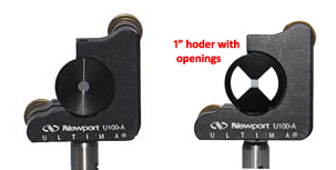
OD 1" crystals can be mounted in a conventional 1" mirror mount to be angle tuned for phase matching (mirror mounts and posts are not included).
BBO Crystal Handling:
BBO has a low susceptibility to moisture. The AR coating or the protective coating (P-coating) on the crystal faces can protect the faces from moisture to some extent. It is fine to leave the crystal in the setup for most optics labs with HR =< 40%. However, we suggest to store the crystal in a desiccator if it will not be used for over > 1 month to prolong the crystal lifetime. Alternatively, a small enclosure (with openings for light) may be built around the crystal with dry nitrogen or air continuously flow into the enclosure. The dry nitrogen/air pressure needs only to be slightly above the atmosphere to keep the small volume around the crystal dry and clean.
BBO is relatively soft and therefore requires precautions to protect the surfaces.
Cleaning the Crystals:
Dust and stains on crystal surfaces can cause scattering/loss of light and can even react with light to damage optical surfaces at a high incident laser power.
You can inspect the crystal surface for dust and stains by holding it near a bright visible-light source. Viewing at different angles helps to see scattering from dust and stains. The crystal surface has to be cleaned if dust and stains are found.
You should perform the following cleaning procedures in a clean, low-dust environment while wearing powder-free gloves or finger cots.
Blowing off the crystal surface
A canister of compressed N2/clean air or a blower bulb (http://www.adorama.com/GTRABS.html ) can be used to blow off dust and other loose contaminants. If a dry nitrogen line is available in the lab, an air gun can also be used to blow away dust particles. Blow off the surface gently. Do not blow off the crystal itself from your hand!
Do not use contact methods to remove dust or stains from the thin crystal surfaces.
 FROGpresentation-by-Trebino (5.15MB)
If you do not find the suitable products above, you may let us know your requirements or applications in the form below. Our sales or technical staff will get back to you as soon as possible.
Please provide your contact information for us to get back to you:
Name:Title:
Organization:
Work Phone:
E-Mail Address:
Enter the code in the box below:
